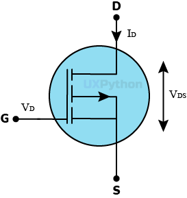
The NTLJS3113P is a P-Channel metal-oxide semiconductor field-effect transistor (MOSFET) is the most common type of field-effect transistor (FET). This transistor has a three-terminal device with Gate (G), Drain (D) and Source (S) terminals.
Circuit diagram symbol of the NTLJS3113P transistor as follows.
| Transistor Code | NTLJS3113P | |
|---|---|---|
| Transistor Type | MOSFET | |
| Control Channel Type | P-Channel | |
| Package | WDFN6 | |
| Drain-Source Voltage (Maximum) | VDS | 20V |
| Gate-Source Voltage (Maximum) | VGS | 8V |
| Drain Current (Maximum) | ID | 7.7A |
| Drain-Source On-State Resistance (Maximum) | RDS(on) | 0.032Ohm |
| Power Dissipation (Maximum) | PD | 3.3W |
| Total Gate Charge | 13nC | |
The NTLJS3113P is a transistor, a MOSFET, used for on and off switching in electrical gadgets and power control applications. It is a P-Channel MOSFET, which means it conducts when a negative voltage is applied to the gate with respect to the source.
This device comes in a WDFN6 package, making it suitable for projects that require low power handling and reliable switching performance.
Followings are the key electrical characteristics of the NTLJS3113P MOSFET transistor
The maximum drain-source voltage that can safely block between drain and source in NTLJS3113P MOSFET transistor is 20V.
This is the highest voltage the MOSFET transistor can safely block between the drain and source without damadging to the transistor.
The maximum safe voltage that can be used between the gate and source of the NTLJS3113P MOSFET transistor is 8V without any harm. This limit should not be exceeded to prevent damage from the gate voltage.
The maximum continuous current flowing between the drain and source of the NTLJS3113P MOSFET transistor is 7.7A. This is the highest current that can safely flow between drain and source without damaging the MOSFET transistor.
The internal resistance between the drain and source of NTLJS3113P MOSFET transistor when the transistor is fully turned on is 0.032 Ohm that defines the amount of lost power that is wasted as heat when the transistor is operating.
The maximum power that the NTLJS3113P MOSFET transistor can comfortably transfer into heat without breaking is 3.3W. This indicates the amount of power that can safely be dissipated to the device as heat.
The time that the drain current or output voltage increases between low to high when the NTLJS3113P MOSFET transistor is switched on is . This is the rate at which NTLJS3113P MOSFET transistor switches on.
This shows how fast the MOSFET transistor switched on.
UXPython is not the creator or an official representative of the NTLJS3113P MOSFET transistor. You can download the official NTLJS3113P MOSFET transistor datasheet to get more infromation about this transistor.
Note : Copyrighted materials belong to their creator or official representative.

Copyright © UXPython inc. All rights reserved.
Devoloped by UXPython.